Investment in high technology start up from as little as £10
Barcelona, Spain – 27 March 2018. Nano-technology Company, Nanusens, has taken an innovative step of crowd funding for a round of investment. Investment starts from as little as £10 on www.crowdcube.com/nanusens
Nanusens CEO, Dr Josep Montanyà i Silvestre, explained: “We have venture capital firms already investing in this round that have been supporting us for a number of years as they believe in our novel technology. I think we are one of the first high technology companies to also offer the opportunity for people to easily invest using the simple process of Crowdcube. We already have 135 investors and raised £131,500 on Crowdcube, which is a 32% of the way to our target.”
Investing via Crowdcube can be done via a credit card payment or PayPal and only becomes effective once 90% of the target figure of £400,000 has been reached at the end of the crowd funding campaign.
Until now, sensors had to come off the standard CMOS production line to have the MEMS created on them using different processes. Nanusens multi-patent pending technology enables it to create nano-sensors using a standard CMOS processes within the same production flow as the rest of the chip production. This innovative approach dramatically reduces the size and cost of the sensors along with up to 85% reduction in the time to market.
“Our first silicon nano-sensor samples from GLOBALFOUNDRIES exceeded our expectations,” explained Dr Montanyà, “with a sensitivity that is an order of magnitude above what is needed for a motion sensor in most applications. The mechanical operation of the nano-sensor design was the tricky part to get right, as that is where the innovation happens. That works perfectly and the design is fixed. Everything from now onwards just involves standard CMOS processes. Partnering with GLOBALFOUNDRIES will ensure good yields and that we will be able to rapidly ramp up production as sales take off. We have a disruptive technology solution that will revolutionise the sensor market and meet the ever-increasing demand for low cost sensors in smartphones, wearable technology and IoT devices that has already made sensors a multi-billion dollar industry.”
Nanusens has the supply chain fully defined, having partnered with trusted providers, like JCAP, member of JCET, the largest assembly group in China. The first product is planned to be ready by September. Upon finishing the electronic part and doing final qualification, sales will start. Nanusens is already in conversations with potential customers in China with whom the final specifications have been defined.

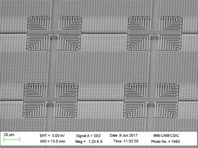
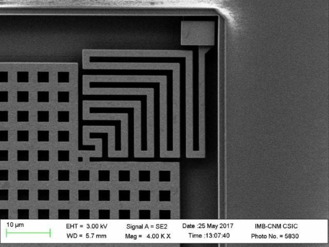
How the sensors are made using standard CMOS processes
The Inter Metal Dielectric (IMD) is etched away through the pad openings in the passivation layer using vapour HF (vHF) to create the nano-sensor structures. The holes are then sealed and the chip packaged as necessary. As only a standard CMOS process with minimal post-processing is used, and the sensors can be directly integrated with active circuitry as required, the sensors can potentially have high yields similar to CMOS devices.
Further details can be seen at https://vimeo.com/258745205
About Nanusens www.nanusens.com
Founded in 2014, Nanusens is pioneering the development of nano-scale sensors that overcome a major problem of MEMS inertial sensors – stiction – by two orders of magnitude by reducing the sensor size by an order of magnitude into the nano-realm. Nanusens is VC funded by Inveready (www.inveready.com/venture-capital/), Caixa Capital Risc (www.caixacapitalrisc.es/en/) and Dieco Capital (www.dieco-capital.com).